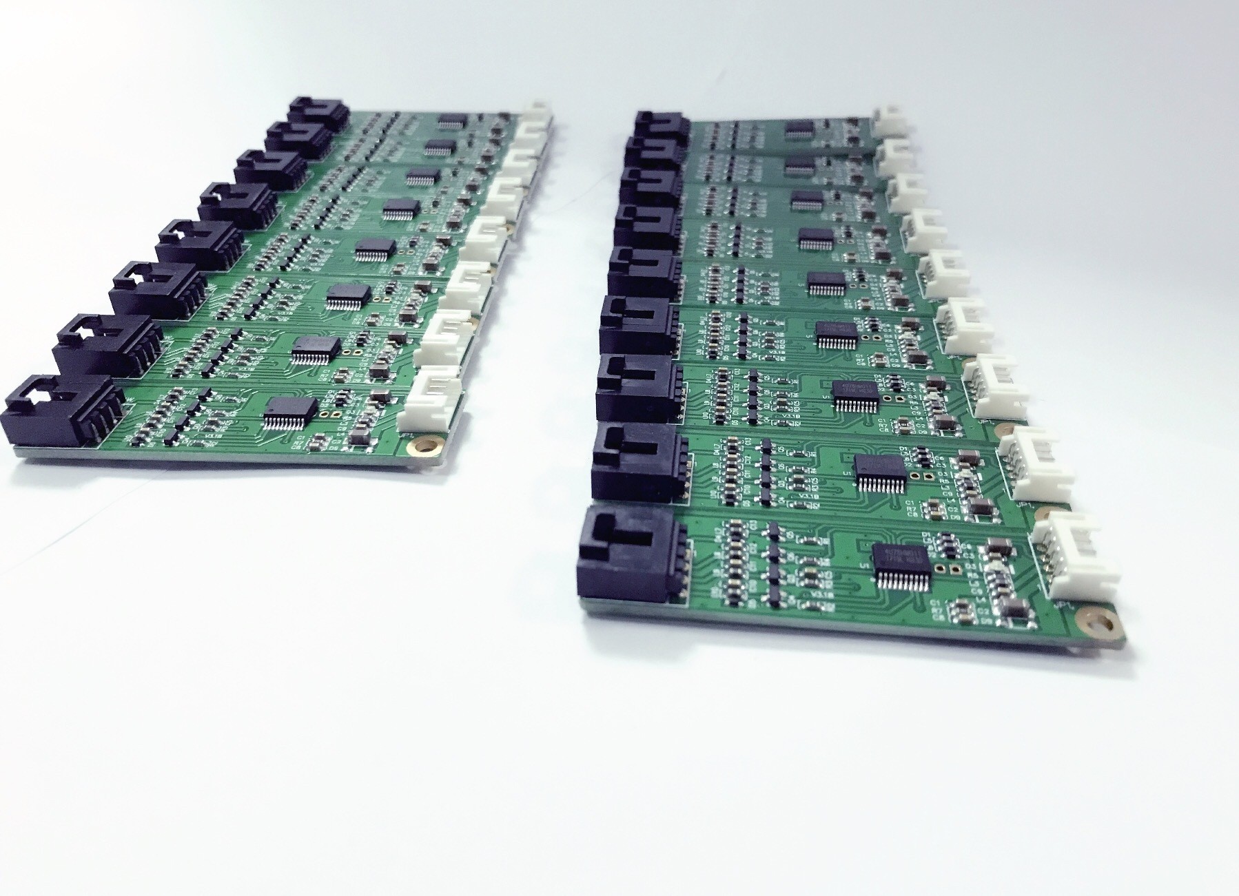
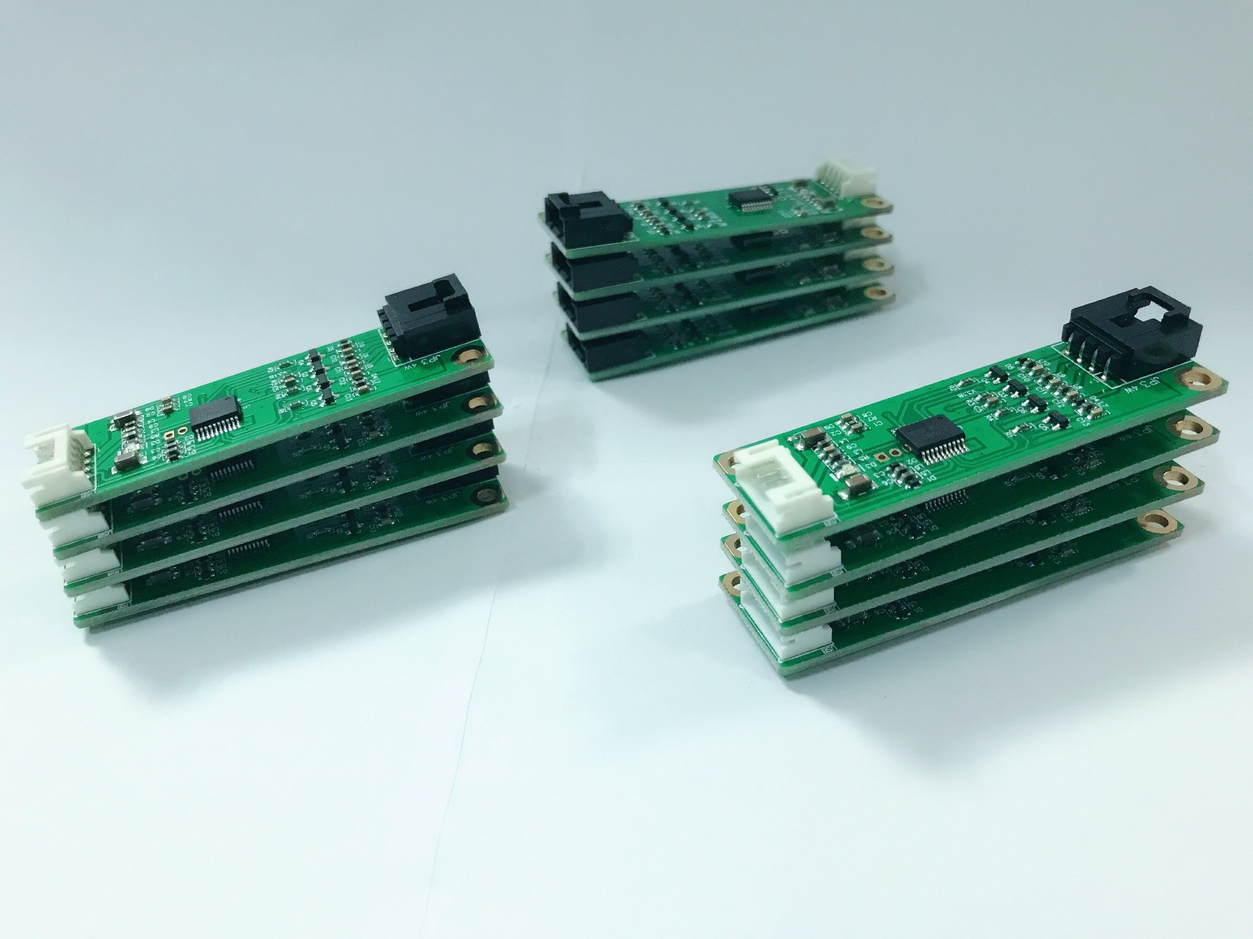
FX-TK05U-VER2.22 B
1
FX-TK05U-V2.22 B USB Controller
Specifications for the TK05U-V2.22 B controller include:
•Electrical
•Environmental
•Physical Characteristics
Electrical
Supply Voltage and Current
•+5 Vdc, nominal (+4.75 to +5.25 Vdc)
•100 mA, typical at +5 Vdc. Average power dissipation is 0.2 W, typical.
•Supply must be capable of sourcing 300 mA, minimum.
•Total noise and ripple requirement must be less than 100 mV (p-p) for frequencies
below 1 MHz, and less than 50 mV (p-p) for frequencies above 1 MHz.
Interface
•Support USB jumper selectable host communication interface.
•USB
oCompliant USB 1.1 low speed device spec.
oSupport suspend and remote wakeup capability
Operating Modes
•Desktop
•Drawing
•Button
Conversion Time
•Max. 200 Points/Sec(pps), typical 160pps
Serial Communication Protocol
•UTCP : Default for USB, Ref. to UTCP reference manual for detail
•MTTM: MT410TM/510TMprotocol,
•EloTM: SmartSetTMprotocol,
Reliability
•MTBF greater than 300,000 hours per MIL-HDBK-217-F2 using the parts stress
calculation b for ground benign environment with an ambient temperature of
25°CFX-TK05U-VER2.22 B
2
Environmental
Temperature
•Operating: 0°C to 65°C
•Storage: -25°C to 85°C
Humidity
•Operating: 10% to 90% RH, non-condensing
•Storage: 10% to 90% RH, non-condensing
Shock and Vibration
•Three axis sine wave, 50 Hz to 2kHz, 1 G, 2 minutes/Octave with dwell on resonances
ESD
•Per EN 6100-4-2 1995: Level 4. Contact discharge 8kV, air discharge 15kV.
Flammability
•The printed circuit board substrate is rated 94V0. All plastic components, such as
headers and connectors, are also rated 94V0.
Physical Characteristics
Construction()
•Four-layer surface-mount design with internal ground plane for EMI suppression.
Dimension
•Total Width: 20 mm
•Total Length: 68 mm(including connectors)
•Total height: 8.3mm
•All mounting holes are plated through for chassis ground connection. Refer to the
drawings at the end of this document.FX-TK05U-VER2.22 B
3
Connectors and Pin Definitions
•The connector configuration permits the controller to be placed in-line between the
touchscreen and serial I/O attachments.
The USB connector,JP1, is a single row by seven-b header with pins spaced on
1mm centers. Refer to the following figure for pin number bs.
Figure 1. Pin diagram for serial connector, J2, as viewed from connector mating
surfaces
Signal definition forUSB
interface JP1
Signal Name JP1 pin
Signal Function
GND 1 signal ground
Power (V5IN) 2 +5V power drain from host USB port
GND 3 signal ground
D+
4 USB bus signal
D- 5 USB bus signal
Table 1. Host Connector, JP1, signal names and functions
Touch screen connector, JP3(JP4)signal debions
The touch screen connector, JP3, is a dual row by five-b header with
0.025-inch square pins spaced on 0.100 centers. 5W sensor must be
connected to the low row of the connector.
The 4 Wire Touchscreen connector, JP3 lower row, and signal debions
Table 2. Touchscreen connector, JP3 lower row, pins and signal names
Signal name
JP3 pin
(JP4)
Signal function
LL 1 5线电阻触摸屏LL
LR 2 5线电阻触摸屏LR
COM 3 5线电阻触摸屏COM(WIPER)
UR 4 5线电阻触摸屏UR
UL 5 5线电阻触摸屏UL


|
深圳市方显科技有限公司
|
|
联系地址:广东省 深圳市宝安区松岗红湖路168号A1栋5楼
联系电话: 朱先生:17674051965
|

